It has been six months since I started doing Schematic design and PCB Layout by myself. I have been working on these things for improving my engineering skills and exhibiting my prototypes in Maker Faire, especially for bone conduction devices that I am developing. I finally could make my own PCB which worked perfectly, so I will show my progress of PCBs.
The first experiment failed…
When I developed my own PCB for the first time, I designed a schematic which was definitely over-skilled for me. Even thought I just wanted to make a PCB which can make sounds through an amplifier, I put BLE for Bluetooth function, and Li-Polymer Charge Management Controller to charge a LiPo Battery. Of course, the PCB did not work because I did not know how to design schematics and PCBs. What I learned from this failure is…
- Do not try to design a complicated PCB for the first time.
- Increase the difficulty of schematic and PCB layout gradually.
- Know how the electronics work better than anybody else.
The second experiment also failed…
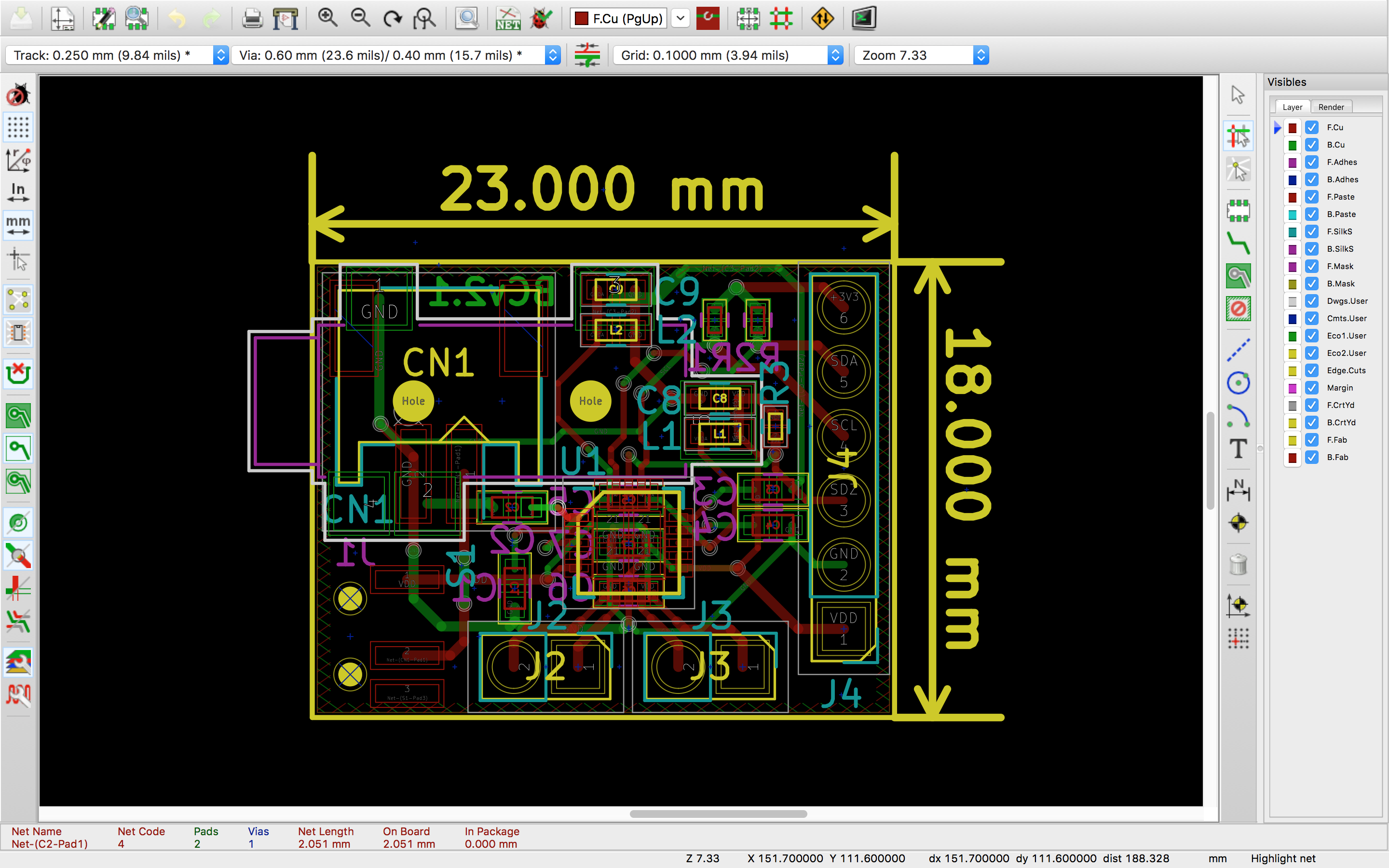
From the first failure, I design a easy PC board by eliminating a lot of functions that I was not supposed to use this experiment. And, this is the schematic that I designed.

However, this schematic also did not work because It had three errors.
- I did not connect Pin 21 (Thermal Pad) on an amplifier to the GND (ground).
- R1, R2, and R3 (resistors) were not working as pull-up resistors.
- INL- (Left channel negative audio input) and INR- (Right channel negative audio input) also did not connect to the GND.
In order to fix these errors,
- Make a hole on pin 21 using laser cutter and solder pin 21 to GND pin using a tiny wire. (The reason why I made a hole was the package of the amplifier was QFN and needed to be soldered using soldering cream and heat gun).
- Connect SDA, SCL, SDZ pins to VDD pin using three jumper wires.
- Connect INL- to GND pin using a jumper wire.
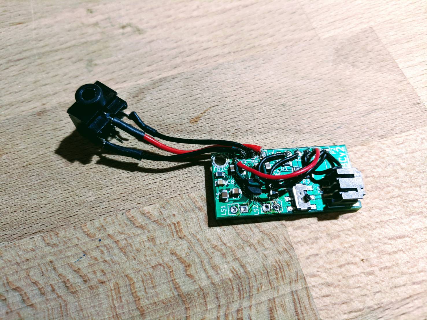
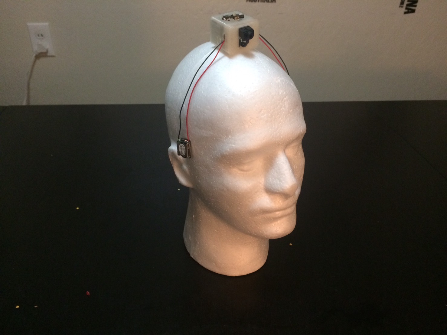
After these debugging, my PCB called BCv2.0 finally worked.
BCv2.1 came out!
From previous failure, I redesigned the schematic.

The PCB became much smaller and practical and I removed the external 3.5mm headphone jack and used SMD headphone jack.
By placing components on both side, I could minimize the size a lot.


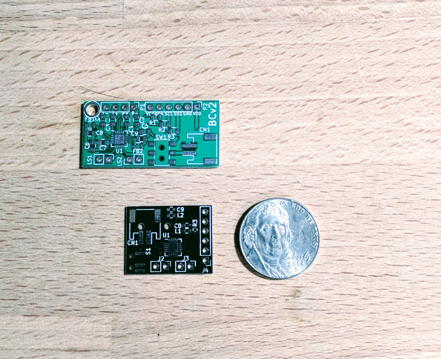
The Size Comparison
I could successfully minimize the size of PCB. This is the comparison of BCv2.0 (Green), BCv2.1 (Black), and 5 cent coin.
Next challenge I will do is to put more functions such as bluetooth on my own PC Board! See you at next post!