Objective
The objective of this post is to implement a 4×4 multiplier using full adders in Verilog. A nxn array multiplication is simply a gathering of a 1-bit node that contains a 1-bit full adder. The node has two outputs in horizontal and vertical, and each output is passing data whether 1 or 0 to the next node horizontally and vertically. In the first row of an array multiplier, it assumes that the vertical inputs are connecting to the ground which means it passes 0 to a node. Likewise, in the first row of an array multiplier, it also assumes that the horizontal inputs are connecting to the ground, so it passes 0 to a node. In the next node that was passed data from the previous node, the horizontal output from the previous node is connecting and the horizontal input to the next node. In addition, if there is no node connected vertically, the data held in the vertical output will return as a result of a bit.
Environment, Tool, and Board
- Ubuntu 16.04
- Vivado 2018.3
- Nexys A7 100T (Family: Artix-7, Package: csg324, Speed: -1L)
- Part: xc7a100ticsg324-1L)
Implementation
In the structural model of the 4×4 array multiplier using full adders in Verilog, 16 nodes should be instantiated in the module. In addition, by assigning the computed output wire after instantiating node to the output which is represented “p”, the Nexys board can physically know what to light up.
|
1 2 3 4 5 6 7 8 9 10 11 12 13 14 15 16 17 18 19 20 21 22 23 24 25 26 27 28 29 30 31 32 33 34 35 36 37 38 39 40 41 42 43 44 45 46 47 48 49 50 51 52 53 54 55 56 57 58 59 |
`timescale 1ns / 1ps module FA1(Cout, S, A, B, Cin); input A, B, Cin; output Cout, S; wire S1, C1, C2; xor(S1, A, B); and(C1, A, B); xor(S, S1, Cin); and(C2, S1, Cin); or(Cout, C1, C2); endmodule module Node1(HCout, VCout, A, B, HCin, VCin); input A, B, HCin, VCin; output HCout, VCout; wire W1; assign W1 = A&B; FA1 fa1(HCout, VCout, W1, VCin, HCin); endmodule module multiplier(p, a, b); input [3:0] a, b; output [7:0] p; wire [3:0] sum0, sum1, sum2, sum3, sum4, sum5, sum6; wire [3:0] c0, c1, c2, c3, c4, c5, c6; // First row Node1 node0(c0[0], sum0[0], a[0], b[0], 0, 0); Node1 node1(c1[0], sum1[0], a[1], b[0], c0[0], 0); Node1 node2(c2[0], sum2[0], a[2], b[0], c1[0], 0); Node1 node3(c3[0], sum3[0], a[3], b[0], c2[0], 0); // Second row Node1 node4(c1[1], sum1[1], a[0], b[1], 0, sum1[0]); Node1 node5(c2[1], sum2[1], a[1], b[1], c1[1], sum2[0]); Node1 node6(c3[1], sum3[1], a[2], b[1], c2[1], sum3[0]); Node1 node7(c4[1], sum4[1], a[3], b[1], c3[1], c3[0]); // Third row Node1 node8(c2[2], sum2[2], a[0], b[2], 0, sum2[1]); Node1 node9(c3[2], sum3[2], a[1], b[2], c2[2], sum3[1]); Node1 node10(c4[2], sum4[2], a[2], b[2], c3[2], sum4[1]); Node1 node11(c5[2], sum5[2], a[3], b[2], c4[2], c4[1]); // Forth row Node1 node12(c3[3], sum3[3], a[0], b[3], 0, sum3[2]); Node1 node13(c4[3], sum4[3], a[1], b[3], c3[3], sum4[2]); Node1 node14(c5[3], sum5[3], a[2], b[3], c4[3], sum5[2]); Node1 node15(c6[3], sum6[3], a[3], b[3], c5[3], c5[2]); assign p[0] = sum0[0]; assign p[1] = sum1[1]; assign p[2] = sum2[2]; assign p[3] = sum3[3]; assign p[4] = sum4[3]; assign p[5] = sum5[3]; assign p[6] = sum6[3]; assign p[7] = c6[3]; endmodule |
Additionally, the constraint file for the 4×4 multiplier can be found on Github designed by Digilent.
|
1 2 3 4 5 6 7 8 9 10 11 12 13 14 15 16 17 18 19 20 21 22 23 24 25 26 27 28 29 30 31 |
# NEXYX A7 Pin Assignments ############################### ## On-board Slide Switches ## ############################### set_property -dict { PACKAGE_PIN J15 IOSTANDARD LVCMOS33 } [get_ports { b[0] }]; #swt[0] set_property -dict { PACKAGE_PIN L16 IOSTANDARD LVCMOS33 } [get_ports { b[1] }]; #swt[1] set_property -dict { PACKAGE_PIN M13 IOSTANDARD LVCMOS33 } [get_ports { b[2] }]; #swt[2] set_property -dict { PACKAGE_PIN R15 IOSTANDARD LVCMOS33 } [get_ports { b[3] }]; #swt[3] set_property -dict { PACKAGE_PIN R17 IOSTANDARD LVCMOS33 } [get_ports { a[0] }]; #swt[4] set_property -dict { PACKAGE_PIN T18 IOSTANDARD LVCMOS33 } [get_ports { a[1] }]; #swt[5] set_property -dict { PACKAGE_PIN U18 IOSTANDARD LVCMOS33 } [get_ports { a[2] }]; #swt[6] set_property -dict { PACKAGE_PIN R13 IOSTANDARD LVCMOS33 } [get_ports { a[3] }]; #swt[7] ############################ ## On-board LEDs ## ############################ set_property -dict { PACKAGE_PIN H17 IOSTANDARD LVCMOS33 } [get_ports { b[0] }]; #led[0] set_property -dict { PACKAGE_PIN K15 IOSTANDARD LVCMOS33 } [get_ports { b[1] }]; #led[1] set_property -dict { PACKAGE_PIN J13 IOSTANDARD LVCMOS33 } [get_ports { b[2] }]; #led[2] set_property -dict { PACKAGE_PIN N14 IOSTANDARD LVCMOS33 } [get_ports { b[3] }]; #led[3] set_property -dict { PACKAGE_PIN R18 IOSTANDARD LVCMOS33 } [get_ports { a[0] }]; #led[4] set_property -dict { PACKAGE_PIN V17 IOSTANDARD LVCMOS33 } [get_ports { a[1] }]; #led[5] set_property -dict { PACKAGE_PIN U17 IOSTANDARD LVCMOS33 } [get_ports { a[2] }]; #led[6] set_property -dict { PACKAGE_PIN U16 IOSTANDARD LVCMOS33 } [get_ports { a[3] }]; #led[7] set_property -dict { PACKAGE_PIN V16 IOSTANDARD LVCMOS33 } [get_ports { p[0] }]; #led[8] set_property -dict { PACKAGE_PIN T15 IOSTANDARD LVCMOS33 } [get_ports { p[1] }]; #led[9] set_property -dict { PACKAGE_PIN U14 IOSTANDARD LVCMOS33 } [get_ports { p[2] }]; #led[10] set_property -dict { PACKAGE_PIN T16 IOSTANDARD LVCMOS33 } [get_ports { p[3] }]; #led[11] set_property -dict { PACKAGE_PIN V15 IOSTANDARD LVCMOS33 } [get_ports { p[4] }]; #led[12] set_property -dict { PACKAGE_PIN V14 IOSTANDARD LVCMOS33 } [get_ports { p[5] }]; #led[13] set_property -dict { PACKAGE_PIN V12 IOSTANDARD LVCMOS33 } [get_ports { p[6] }]; #led[14] set_property -dict { PACKAGE_PIN V11 IOSTANDARD LVCMOS33 } [get_ports { p[7] }]; #led[15] |
Simulation
|
1 2 3 4 5 6 7 8 9 10 11 12 13 14 |
`timescale 1ns / 1ps module tb(); reg [3:0] a, b; wire [7:0] p; mult4 dut(p, a, b); initial begin a[3]=1; a[2]=1; a[1]=1; a[0]=1; b[3]=1; b[2]=1; b[1]=1; b[0]=1; #50 $stop; end endmodule |
Based on the simple testbench, the binary multiplication of 1111×1111 will be 11100001. Therefore, the p[7] (led[15]), p[6] (led[14]), p[5] (led[13]), and p[0](led[8]) will be 1 (HIGH) on the simulation.

Result
In order to compare the simulation with the result of an actual FPGA board, it tests by generating bitstream.
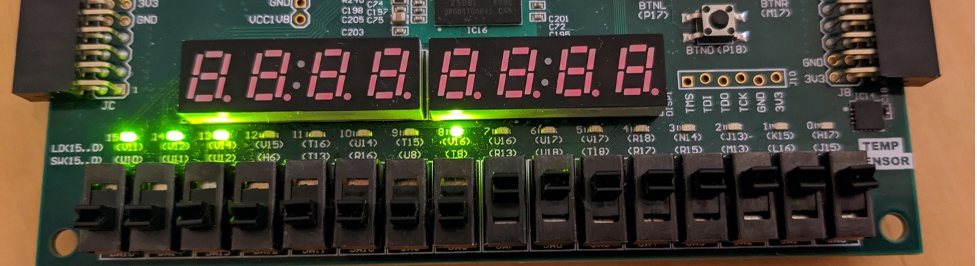
As observed here, when all the swt[7]~swt[0] is on, the actual result of the binary multiplication obtained the expected result.
DONE! Please let me know if you have any questions.